Lecture 7 | The Processor-Part1 Cont.
Chap4 The Processor-Part1
如何实现读取指令与运行
Instruction Execution Overview
两个前置步骤
三种指令类型
- For every instruction, the first two step are identical
- Fetch the instruction from the memory
- Decode and read the registers
- Next steps depend on the instruction class
- Memory-reference
- Arithmetic-logical
- branches

An overview of Implementation
一个处理器的概念图,不是真正的样子
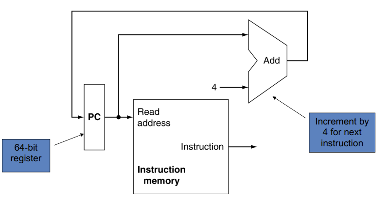
从取址开始,也就是从PC开始
指令在instruction memory里
注意指令固定是32bit
- Send PC to the code memory.
- Read one or two register.
注意,取出来的指令放到reg后还经过了ALU
这是因为load和store有基地址和偏移量
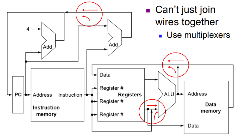
24(x10),需要进行计算两条线交汇处(打红圈的地方)不能直接连接,因为数据不同可能冲突
需要使用Multiplexers
不同指令下怎么选Multiplexers是考点
- Control the units: Read Memory, Write Memory.
mux通过控制线路控制
约定熟成,黑的是数据线,蓝的是控制线
上面zero和branch与了一下,是因为zero的输出不受branch的影响
4.3 Building a Datapath
Execution in RISC-V
- Fetch
- Take instructions from the instruction memory
- Modify PC to point the next instruction
- Instruction decoding & Read Operand:
- Will be translated into machine control command
- Reading Register Operands, whether or not to use
- Reading Register Operands, whether or not to use
- Executive Control
- Control the implementation of the corresponding ALU operation
- Memory access
- Write or Read data from memory
- Only ld/sd
- Write results to register
- If it is R-type instructions, ALU results are written to rd
- If it is I-type instructions, memory data are written to rd
Fetching
涉及三个组件及其连接
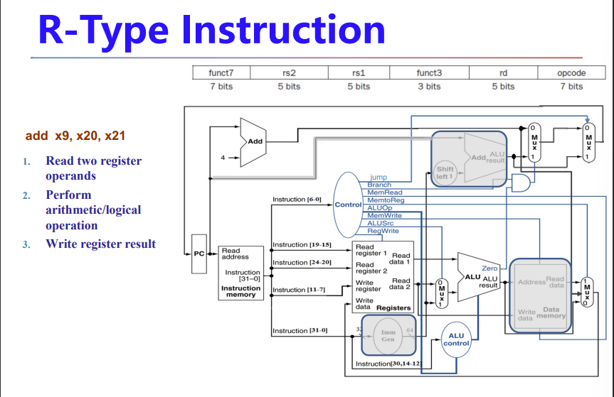
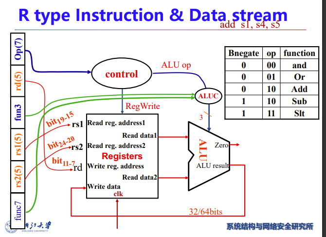
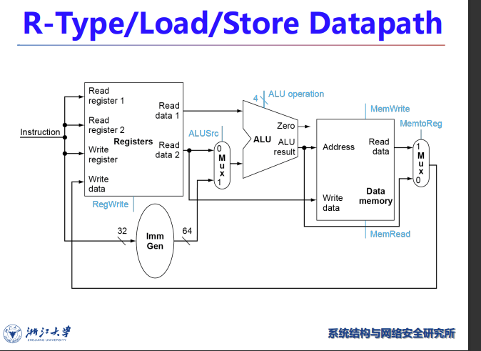
R-Format Instructions
加减法
- Read two register operands
- Perform arithmetic/logical operation
- Write register result
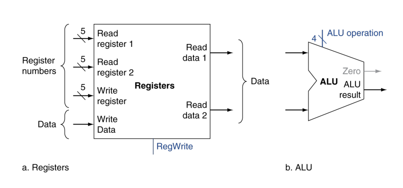
左边这个就是实验写的RegFile
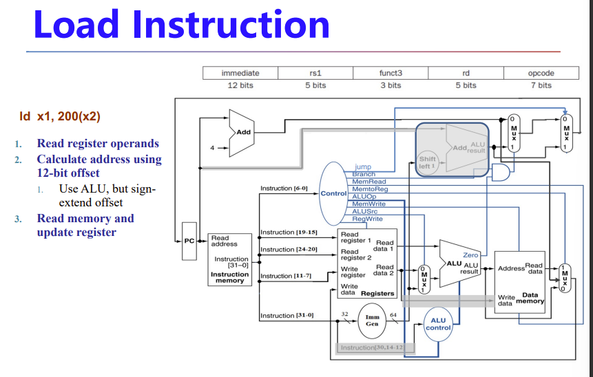
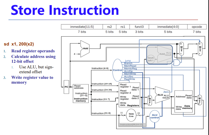
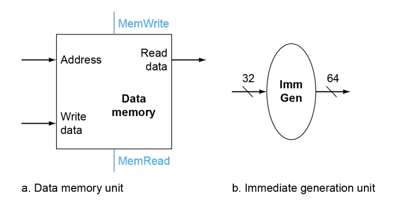
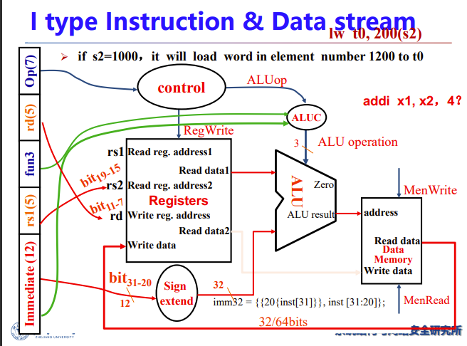
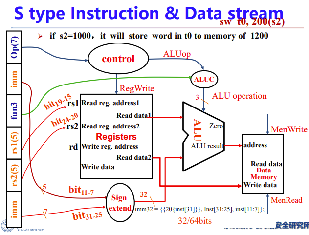
Load/Store
- Read register operands
- Calculate address using 12-bit offset
- Use ALU, but sign-extend offset
- Load: Read memory and update register
- Store: Write register value to memory
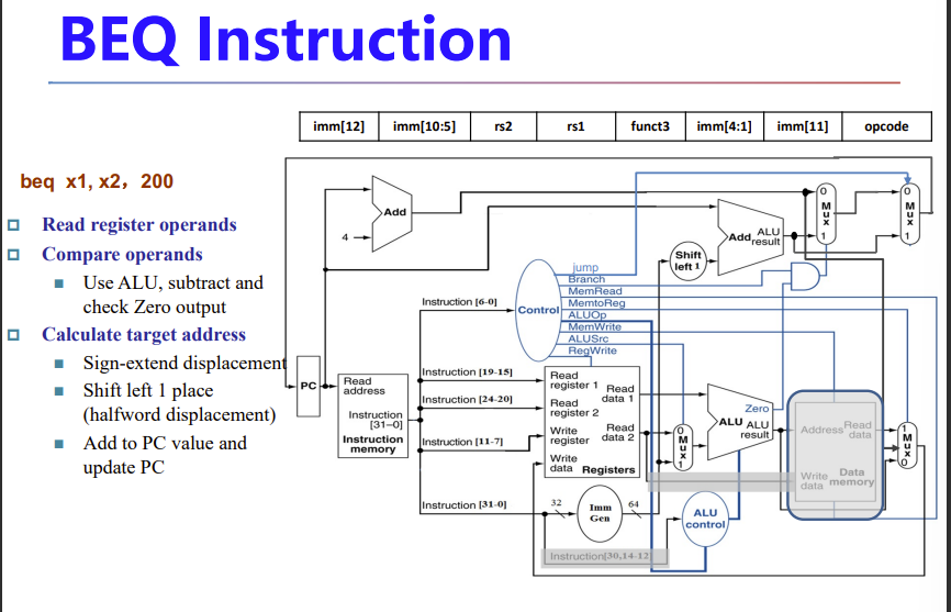
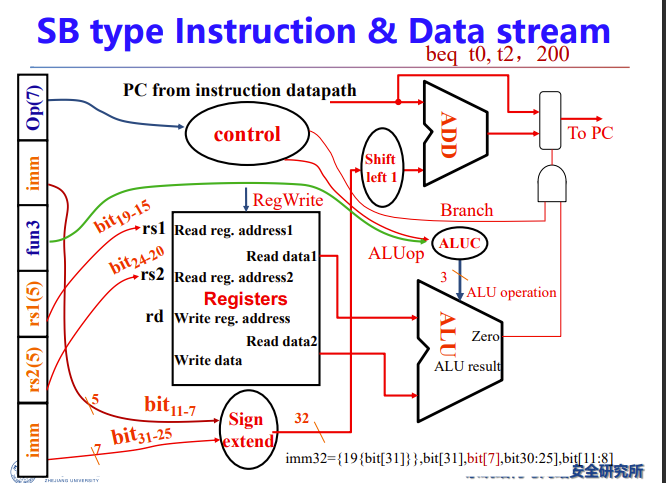
Branch
- Read register operands
- Compare operands
- Use ALU, subtract and check Zero output
- Calculate target address
- Sign-extend displacement
- Shift left 1 place (halfword displacement)
- Add to PC value
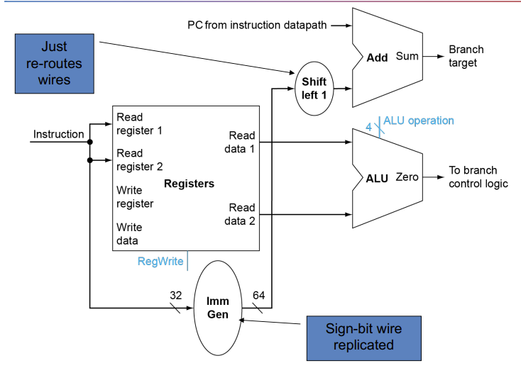
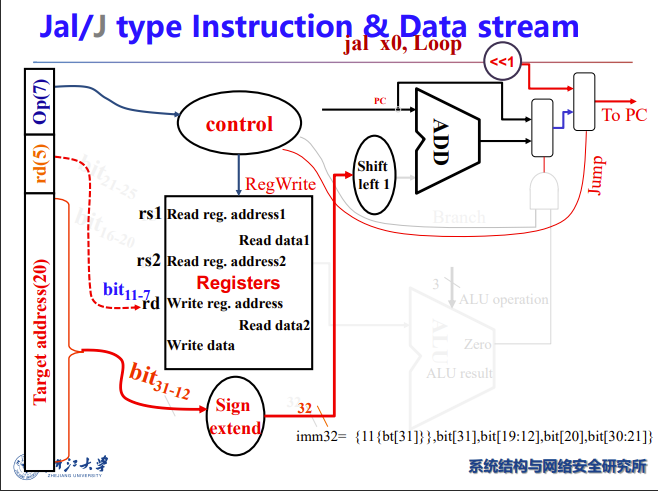
sl 1 是因为RISCV最小支持16bit双字节指令,左移1bit以人为扩大一倍寻址空间而不超过32bit
之前提到过,指令里面imm不是从0位开始而是从1位开始
Composing the Elements
组合上面这些模块
注意
- First-cut data path does an instruction in one clock cycle
- Each datapath element can only do one function at a time
- we need separate instruction and data memories
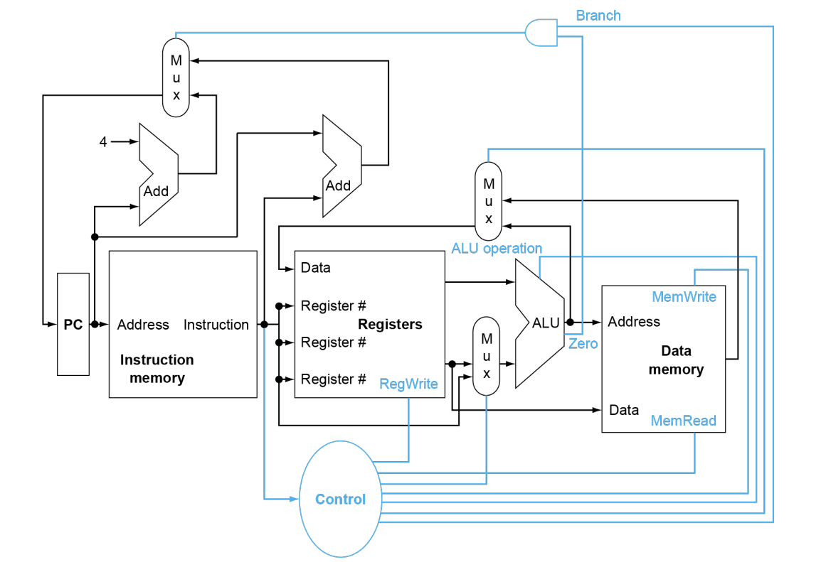
- Use multiplexers where alternate data sources are used for different instructions
Path Built using Multiplexer
从左边的指令出发,指令各部分看连线就很清晰了
这部分着重看指令机器码不同部分的去向
连线看后面部分
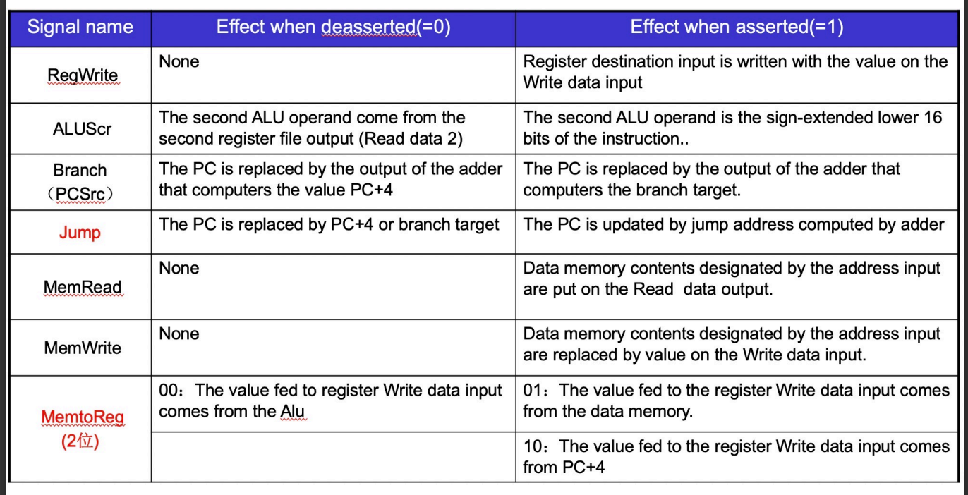
共6个控制信号:
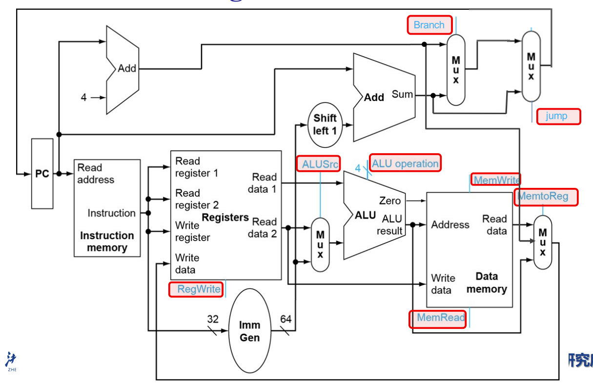
!!!!!Full Datapath!!!!!
要背,会让你直接画出来
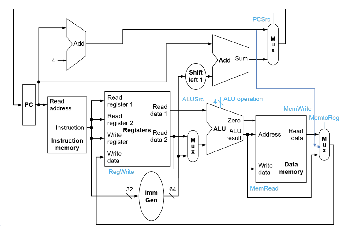
R型指令负责逻辑运算
红色框是解码部分
先通过pc的地址取指令
然后解码,解码后将相应的码位输出到对应的地方
这里将读的地址和写的地址交给了registers,后者将对应地址的数值给ALU
Registers到ALU有一个通路有mux,由ALUSource控制,用于选取立即数或Registers的值
ALU计算完执行写回操作
右下角的mux有2bit控制信号,图里少了个jump指令返回pc+4的输入
menWrite和menRead默认情况下都要强制置零,前者为了避免误写入(这是不可逆的),后者实际上其实无所谓,但是后面会提到,其与cache有关
branch也是强制置零,防止pc被改掉
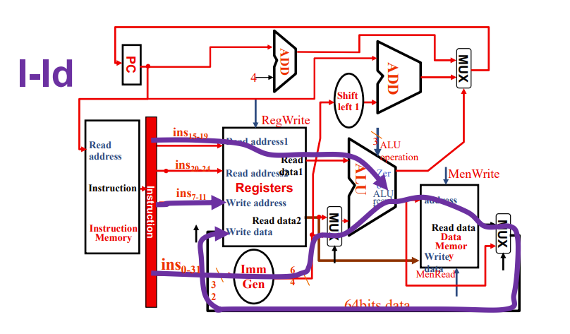
下面讲的是I型指令的ld指令
ld从寄存器取基地址,加上一个立即数的偏置量,由此算出内存的物理地址,然后从mem取数并放回reg
ImmGen用于处理指令里的立即数,比如合并、移位
两个mux与R型都不一样了,且需要进入data mem
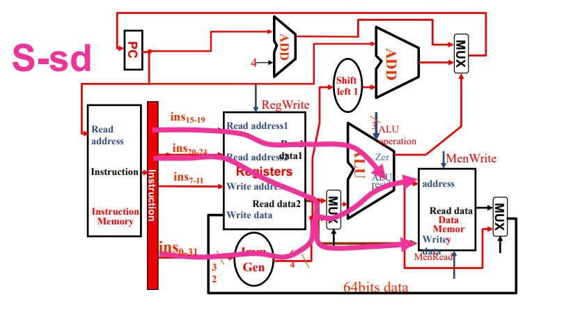
S型指令的sd指令
看上去和ld差不多,基地址、偏移量、数据三元素
但是被分为不同类型的指令,因为涉及两个reg,一个放数据,一个放基地址
而且不用写回,在data mem就结束了
上面都是在reg结束
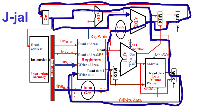
跳转就复杂了,三面上个都长得差不多
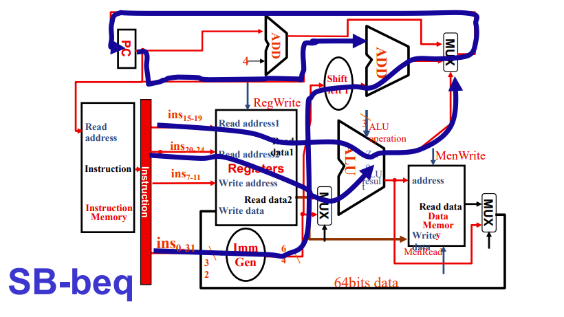
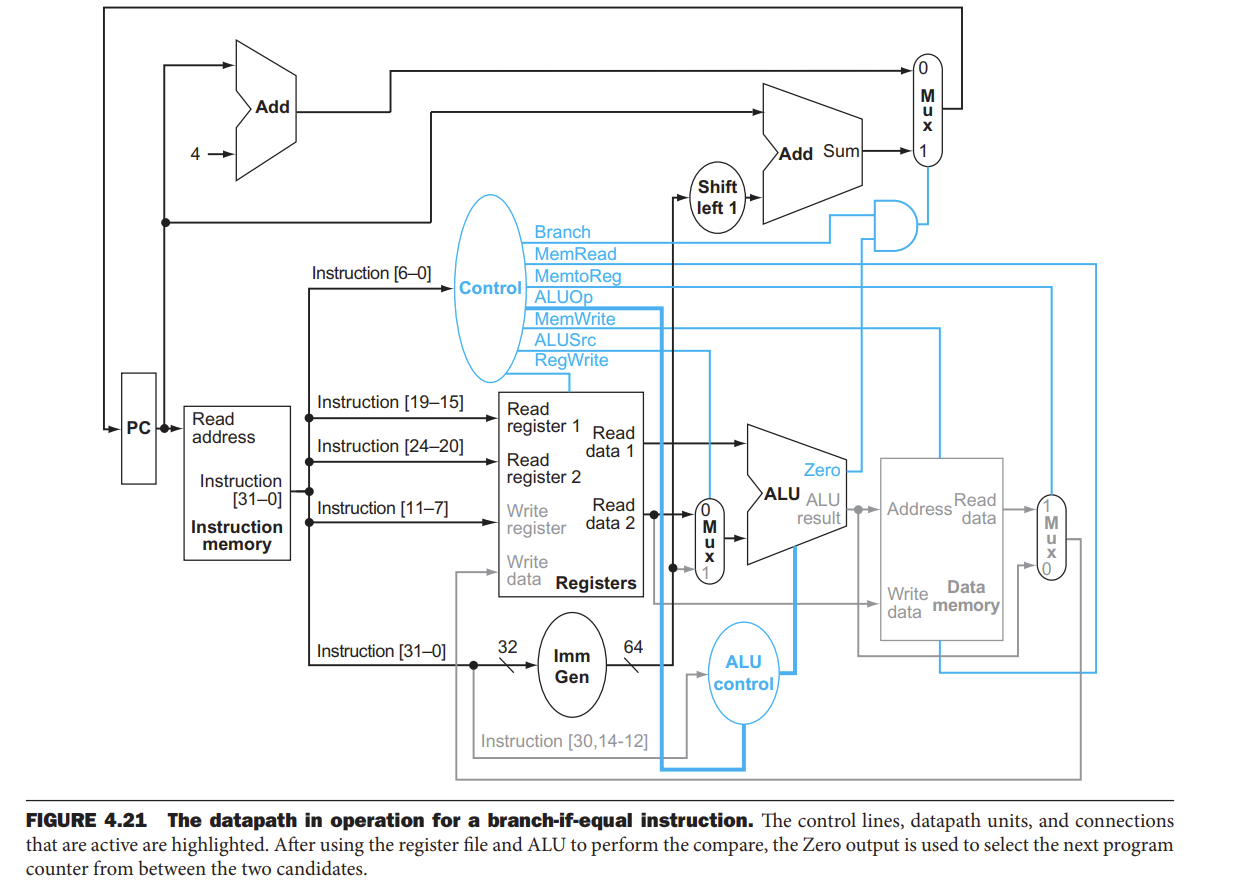
SB类型的beq条件跳转
减法,通过ALU的zero输出判断两个数是否相等
然后立即数左移了一位,因为,beq指令中的imm是地址偏移量,其大小据决定了能跳多远,即寻址范围更大
最低位直接舍去了
实际连线时会直接从第二位开始连,不用额外的移位运算,图中只是强调一下
上面有两个add,左边专门pc+4,右边获得偏移后的目标地址
目标地址会直接给pc,结束beq
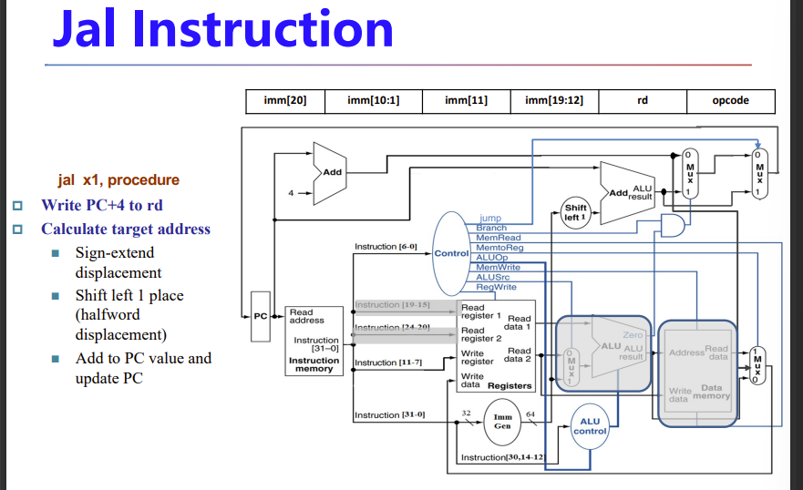
jal书上没讲
Building Controller
There are 7+4 signals
- 7个控制信号
- 4个ALU操作信号
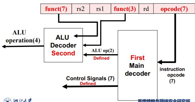
Scheme of Controller
控制信号就是一串二进制数,需要组合电路进行解码
我们分主次两个解码器
- First: Main
- Second: ALU
Truth tables & Circuitry of main Controller
所有的控制信号及其线路
这个图需要记忆,特别是数据线路和控制线路是怎么连线的
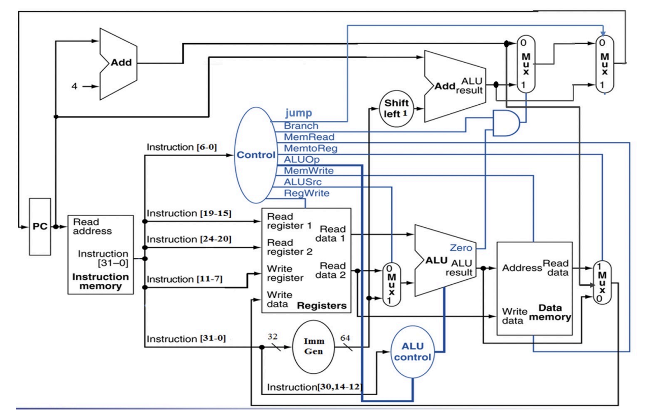
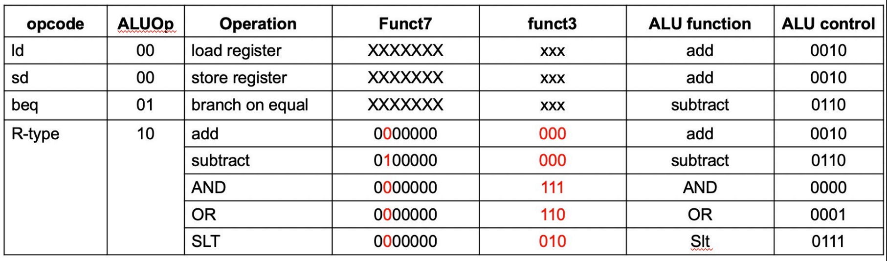
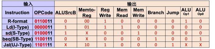
不同指令类型的opcode以及相应的控制信号
会考,要记
the ALU Decoder
ALU operation is decided by 2-bit ALUOp derived from opcode, and funct7 & funct3 fields of the instruction