Cache
第四章的inst mem和data mem实际上就是兩個cache
每一个下层的数据唯一地出现在cache里面,不会重复占用cache地址
注意KB的B是byte,不是bit
KiB是1024 byte
KB是1000 byte
Four Questions for Memory Designers
- 下层数据该映射到上层的什么位置(Block placement)
- 怎么确认下层数据已经在上层(Block identification)
- miss的时候怎么办(Block replacement)
- 写该如何实现(Write strategy)
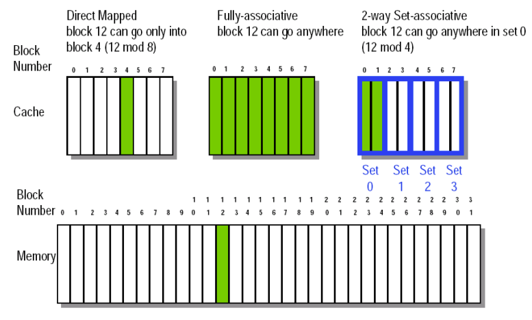
Q1: Block Placement
- Direct mapped Cache
- Block can only go in one place in the cache
- Fully associative Cache
- Block can go anywhere in cache.
- Set associative Cache
- cache的blocks分为多个set
- mem的block固定配对一个set,可以到这个set里面的任意cache block
- fully associative is m-way set-associative (for a cache with m blocks)
- direct mapped is 1-way set associative
Q2: Block Identification
- Tag
- Valid bit
Q3: Block Replacement
直接映射cache 能直接解决这问题,另外两个需要看看set或cache满了该选哪个block来替换
- Random replacement
- Least-recently used (LRU)
- 就是将最久没用的换出去,刚进来的不换
- MRU
- LRU反过来的策略,刚进来的先换出去
- First in,first out(FIFO)
LRU严格的实现比较麻烦
我们可以定期对valid清零,以此表示很久没用了
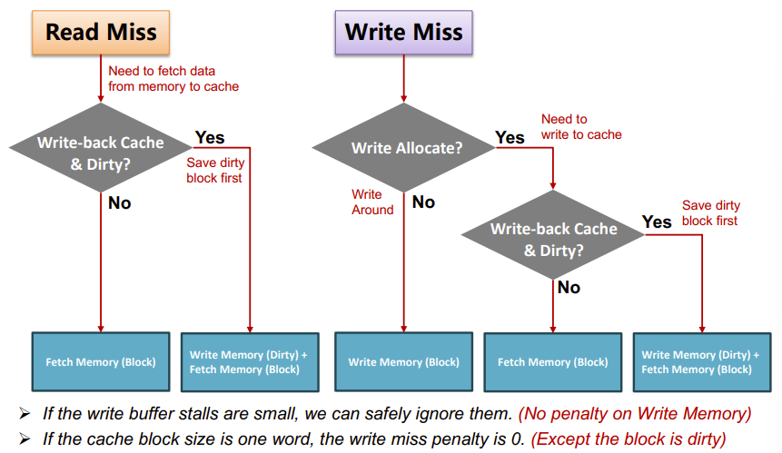
Q4: Write Strategy
write有两种策略
- write-back cache
- 先只更新cache,累计一定更新后一起写到mem,减少mem操作,很快,但会导致不一致
- 有个问题是cache里数据写了却还没放回mem,需要进行保护
- 我们加一个 dirty bit 来标记这种entity
- 即,write-back cache 比 write-through cache 多一bit
- 由此导致效率更高,但是设计更复杂
- write-through cache
- 同时写入cache和mem,每次都要操作mem,所以比较慢
Write Stall
内存写操作很耗时,像 write-through cache 这样每次都往内存写,会造成大量的 Write stall
- Write stall --When the CPU must wait for writes to complete during write through
- 可以加一个 write buffer 减小stall造成的损失
- Write buffer 是位于 CPU和mem之间的一个 small cache
- CPU写出会往 cache 和 Write buffers 一起写,然后让这个buffer来消化写出操作
- 经常用于 write-through cache
- 可以加一个 write buffer 减小stall造成的损失
Write Misses
发现cache里面没有要进行修改的block
- Write allocate
- 先从mem读入cache,再写
- Write around / No write allocate
- 不写cache,用 Write buffers 直接写入mem
In general, write-back caches use write-allocate ,
write-through caches use write-around
Read misses
read 有两类miss
- instruction cache miss
- 遇到时processor会将PC-4这个地址交给mem,将相应的inst重新读入inst cache,再重新执行这指令
- data cache miss
- 就从下层取上来
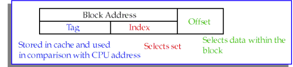
The Format of the Physical Address
这里的index,m,n,tag,都是CPU提供的物理地址被cache解码用到的概念
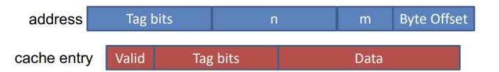
block addr = tag+index
byte addr = tag+index+m+byte offset
两者不要搞混了,线路里传输的地址都是byte addr,block addr是从中抽取的
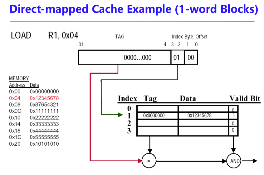
Direct Mapped Cache
取 block addr 的低 \(n\) 位作为 cache 内的地址,一样的在一起
\(n\) 取决于cache有 \(2^n\) 个index
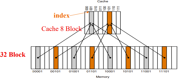
至于怎么区分cache block里面的数据,我们可以通过剩下高处的位作为判断,这些剩下的高处的地址位叫做 \(tag\)
有些block没有data,我们用 valid bit,1表示present,0表示 no present,初始化为0
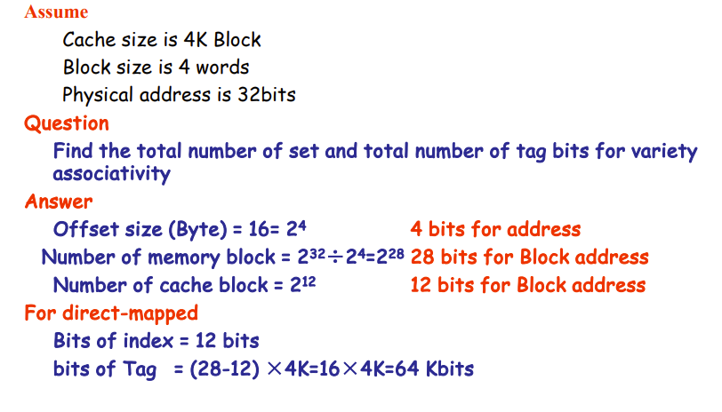
看下tag bits和cache size怎么计算
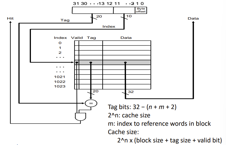
n是index位数
\(2^m\) 是一个block有多少个word,
m+2占的位用于在cache的data里面找到需要的byte,m用于找到block里面的word,2是byte offset 位数用于找到word里面的byte(一个word有4个byte,只需要两bit寻址)
注意,index在 direct-mapped cache 指示 cache entry,在 set-associative cache 指示 set
三类cache示意图
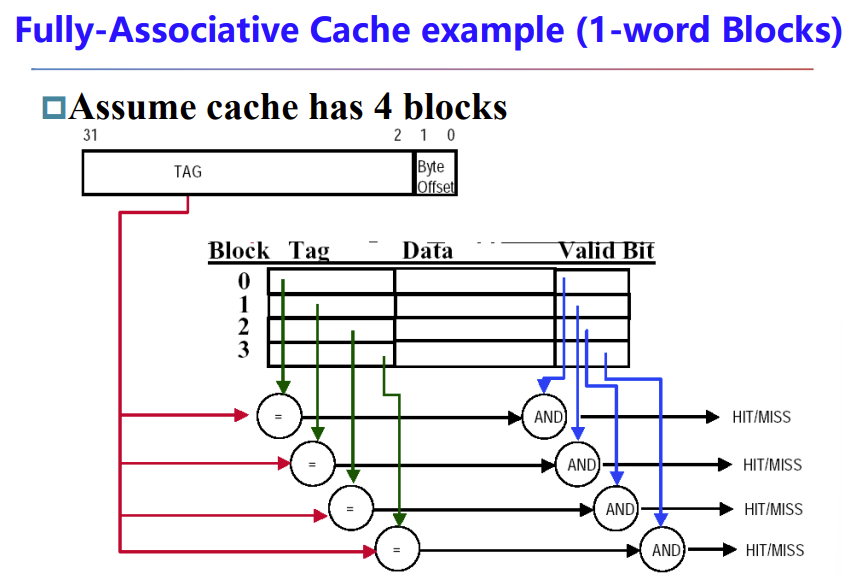
fully associative 采用了并行比较,并行检查所有cache entity的tag和valid bit
注意这种cache解码时物理地址没有分配index,因为这里replace的标准是空闲的就用
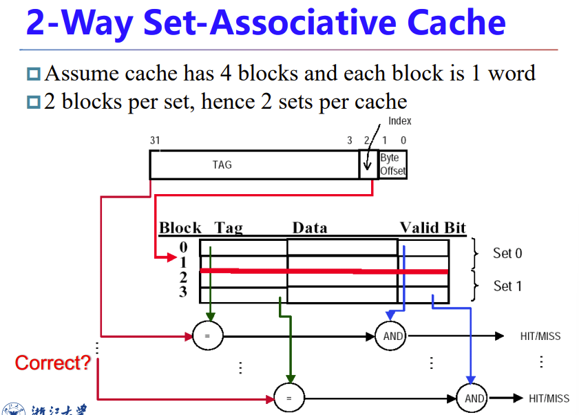
index指示set,所以这图有问题,寻址应该寻的是set,而不是block
这图还有个问题,set确定后只需要检查这个set里面entity的valid bit即可
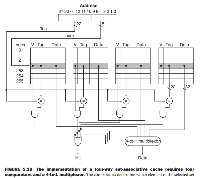
下面这张图要会画,这是一个 4-way set cache
使用到了一个 4to1 的 mux
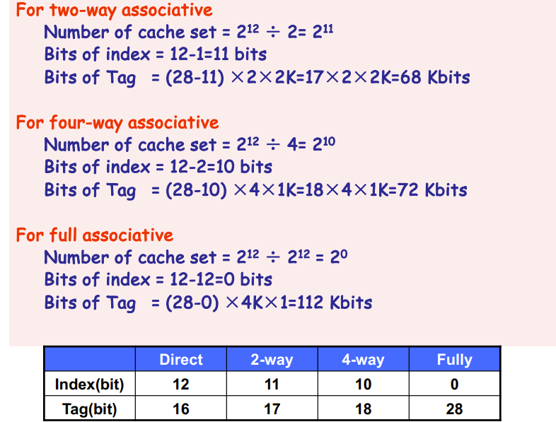
Size of tags versus set associativity EXP
Measuring and improving cache performance
Concept
- Average Memory Assess Time (AMAT) = avg hit time + avg miss time = avg hit time + miss rate × miss penalty
- Hit time
- check hit/miss + cache to CPU
- miss penalty
- mem to cache + cache to CPU
Measuring cache performance
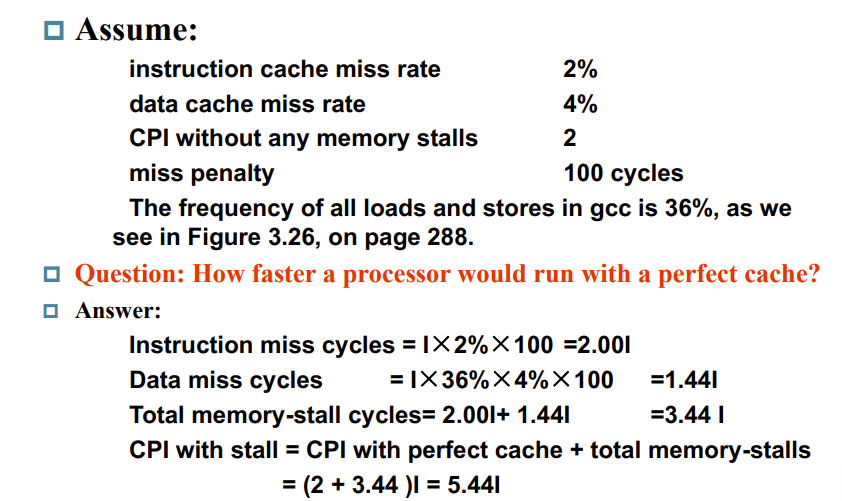
之前学过 CPU_time = Inst ×CPI × Clock cycle time,这个是CPU通畅的总执行时间
但是考虑内存后,因为 mem-stall 会让CPU等待,增加了总的CPU耗时,我们要加上mem的cycle
- CPU time = CPU execution clock cycles + Memory-stall clock cycles
- Memory-stall clock cycles = # of (mem) insts × miss ratio × miss penalty
- = Read-stall cycles + Write-stall cycles
- Read-stall cycles = read指令占总指令的比例 \(*\) read miss rate \(*\) read miss penalty
- Write-stall cycles = write指令比例 \(*\) write miss rate \(*\) write miss penalty + write buffer stall
If the write buffer stalls are small, we can safely ignore them .
If the cache block size is one word, the write miss penalty is 0 ????????
read miss penalty 和 write miss penalty 一般都一样,统一为 mem access penalty,两类指令也统称 mem accesses inst,两类rate也统称 miss rate
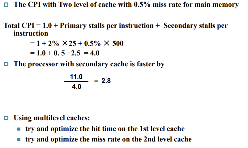
Decreasing miss penalty with multilevel caches
增加一个 二级缓存(second level cache),降低miss
use SRAMs to add another cache above primary memory (DRAM)
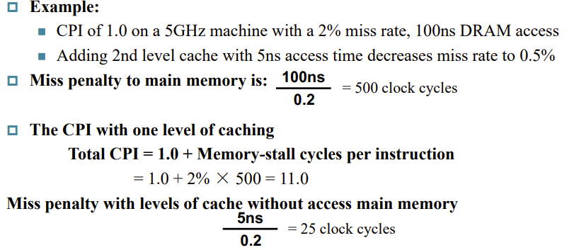
在一些例题里面,miss panlty会省略读取cache的时间,因为很小,实际上应该要包含的
For the given configuration, the possible buffers needed between L1 and L2 caches are: - Write buffer: Since L1 is write-through, a write buffer is needed to hold the data being written to L2 cache. - Read buffer: To hold the data being read from L2 cache to L1 cache. Between L2 cache and memory, the possible buffers needed are: - Write buffer: Since L2 is write-back, a write buffer is needed to hold the data being written to memory when a dirty block is replaced. - Read buffer: To hold the data being read from memory to L2 cache.